Materials and Processing
Rensselaer microelectronics researchers are developing new materials and processes for improved channel, interconnect, and dielectric performance and scaling. With access to our Class 100 cleanroom, they are defining new methods for 3D packaging and heterogeneous integration; leveraging new materials for new technologies, including high power and photonics integration; and devising new metrology methods for relevant materials structure and properties.
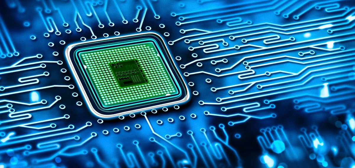
As chip design approaches maximum density, new materials and processes are necessary to optimize performance and functionality while minimizing feature sizes.
Researchers develop new materials and techniques to improve chip performance, reliability, and resistance to damage.
To envision the next generation of microelectronics, researchers harness the computing power available at RPI to predict outcomes and problems in design, manufacture, and function.
With 50 billion transistors on a single chip, researchers strive for more precise measurements and imaging techniques, and for new ways of taking and predicting those measurements.
The next great advancement in semiconductor development will require a new conception of the dimensions of the chip itself.
Researchers apply advances in semiconductor device fabrication to high-power electronics, RF and THz photonics, microelectromechanical systems (MEMS), and biological tissues and sensors.
More efficient and sustainable fabrication will also lead to overall efficiency and sustainability across multiple industries through modeling, analytics, and automation.
Our overarching focus is to promote environmentally responsible semiconductor manufacturing by evaluating the impact of increased chip production on the environment, developing mitigation strategies, exploring new sustainable chemistries for semiconductor processing, and optimizing the use of natural resources.